Take a Look at the New Nvidia Pascal Architecture
Samuel Wan / 8 years ago
With the reveal of the Tesla P100, Nvidia has taken the wraps off of their new Pascal architecture. Originally set to debut last year, delays with 16nm kept Pascal from being a reality, leading to Maxwell on 28nm. Now that Pascal is finally here, we are getting an architecture that combines the gaming abilities of Maxwell with much improved compute performance. The new Unified Memory and Compute Pre-Emption are the main highlights.
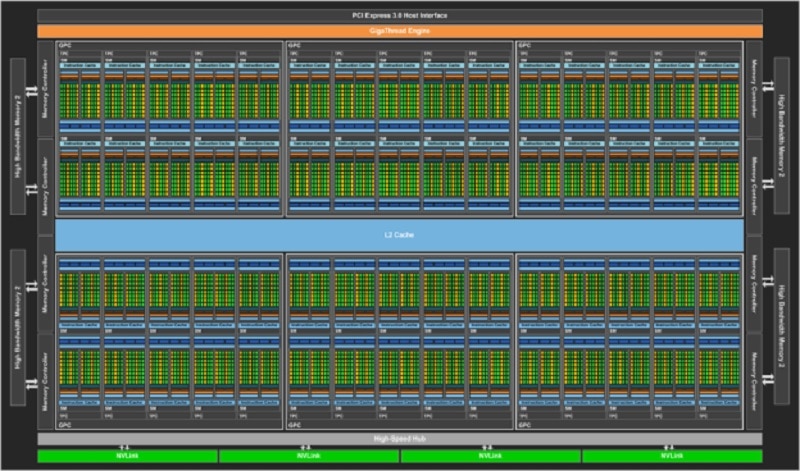
First off, Pascal changes the SM (Stream Multiprocessor) configuration yet again. Kepler featured 192 CUDA cores per SM, Maxwell had 128 and Pascal will now have 64. By reducing the number of CUDA cores per SM, it increases the fine grain control over compute tasks and ensure higher efficiency. Interestingly, 64 is also the same amount of cores GCN has in each CU, AMD’s equivalent to SM. The TMU to CUDA core ratio remains the same as Maxwell with 4 per SM instead of 8, in line with the drop in cores/SM.
For compute, the gains mostly come from increasing the number of FP64 or Dual Precision CUDA cores. DP is important for scientific and compute workloads though game rarely make use of them. Kepler started cutting out some FP64 units and Maxwell went even further, with virtually no FP64 even in the Tesla’s. This was one reason why Maxwell cards were so efficient and Nvidia only managed to hold onto their leadership in compute due to CUDA and their Single Precision performance.
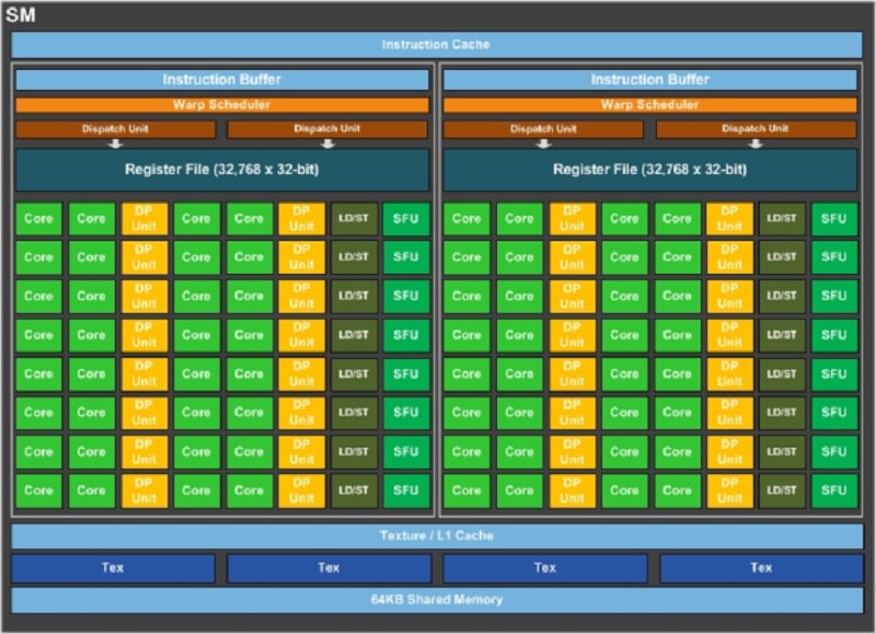
With Pascal, the ratio of SP to DP units goes to 2:1, significantly higher than the 32:1 of Maxwell and 3:1 of Kepler. GP100 in particular has about 50% of its die space dedicated to FP32, about 25% to DP and the last 25% split between LD/ST and SFUs. This suggests that Pascal won’t be changing much in terms of gaming performance. The only gains will be from a slight increase in efficiency due to the smaller SMs and the die shrinking from 16nmFF+. GeForce variants of Pascal may have their FP64 units trimmed to cram in more FP32 resources but again, most of the gains will be due to increased density.
Lastly, Pascal brings forward unified memory to allow threads to better share information. This comes along with improved L2 cache sizes and the more than double register file sizes. P100, the first Pascal chip, also uses HBM2, with 16GB of VRAM over a 4096bit bus for a peak bandwidth of 720 GB/s. For CUDA compute tasks, a new Unified Memory model allows Pascal GPUs to utilize the entire system memory pool with global coherency. This is one way to tackle AMD’s advancement with HSA and GCN and Intel’s Xeon Phi’s.
Overall, Pascal looks to be an evolutionary update for Nvidia. Perhaps, Nvidia has reached the point that Intel has, making incremental progress. In other ways though, the reduction in SM size has great potential and provides a more flexible framework to build GPUs. Now all we are waiting for is for the chips to finally drop.