AMD’s Official Roadmaps Reveals the Company’s Plans for the next 5 Years
Gabriel Roşu / 9 years ago
![]()
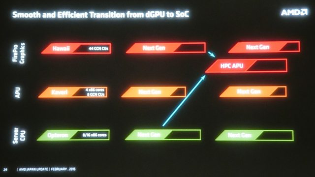
AMD has revealed what the company plans to do with its GPUs and CPUs in the next 5 years at the PC Cluster Consortium event in Osaka Japan, where AMD’s Junji Hayashi revealed the company’s roadmap.
During the event, AMD has focused on its graphics IP and the products that involved it, including discrete Radeon graphics cards and Radeon powered Accelerated Processing Units. There have been talks about AMD’s upcoming K12 ARM as well as the x86 Zen CPU core, including a strategy of how the company plans to introduce both x86 and ARM powered SOCs to the market in a pin for pin compatible platform code-named SkyBridge.
It is said that both CPUs are 64-bit capable parts coming in a 14nm FinFET ‘shell’, but one is based on the ARMv8 architecture while the other is based on the more traditional x86 AMD64 architecture, having them target the server, embedded, semi-custom and client markets.
AMD has also talked about “many threads” revealing that the K12 will come with Simultaneous Multi-Threading (SMT) technology in contrast to the company’s Clustered Multi-Thread (CMT) technology we are able to see in the Bulldozer family. SMT essentially takes advantage of the various resources in the core which are underutilized and dedicate to an additional, slower, execution thread for added throughput. In contrast, CMT is looking for opportunities to share resources between two different CPU cores, instead of doing it inside a single CPU core.
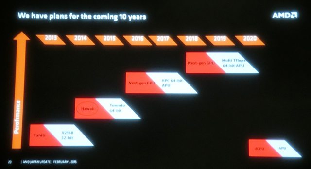
Hayashi also revealed AMD’s GPU roadmap, which reveals that the company is employing a two-year cadence to updating its GPU architecture inside APUs. It looks like the company will add Accelerated Processing Units with updated GPU architectures once every two years. The roadmap also reveals that AMD plans to introduce what it described as a High Performance Computing APU which carries a 200 – 300 watts TDP, having the company stating that the APU in question will excel in HPC applications.
AMD apparently did not attempt to go with newer APUs in the future because it was not viable in terms of memory bandwidth. Instead, the company’s stacked High Bandwidth Memory will be used as an alternative, making the design extremely effective. The second generation of HBM is said to be 9 times faster than GDDR5 memory and 128 times faster than DDR3 memory.
The company has not revealed any code names for the GPU architectures, but a previous leak pointed out that the architecture will debut on 16nm FinFET and will be code-named Arctic Islands. More specific details about AMD’s products will be revealed in May at the Financial Analyst Day event.
Thank you WCCF for providing us with this information