Ivy Bridge Die Layout Estimated
Peter Donnell / 12 years ago

Hiroshige Goto, contributor for PC Watch that is known for detailed schematics of dies estimated the layout of Ivy Bridge silicon. Ivy Bridge is Intel’s brand new multi-core processor silicon built on its new 22 nanometer silicon fabrication process. The four core silicon, which four configurations can be carved, will be built into packages that are pin-compatible with today’s Sandy Bridge processors. The die area of Ivy Bridge is 160 mm², it has a total transistor count of 1.48 billion, compared to the Sandy Bridge silicon, which has 1.16 billion transistors crammed into a die 216 mm² in area, built on the 32 nm process.
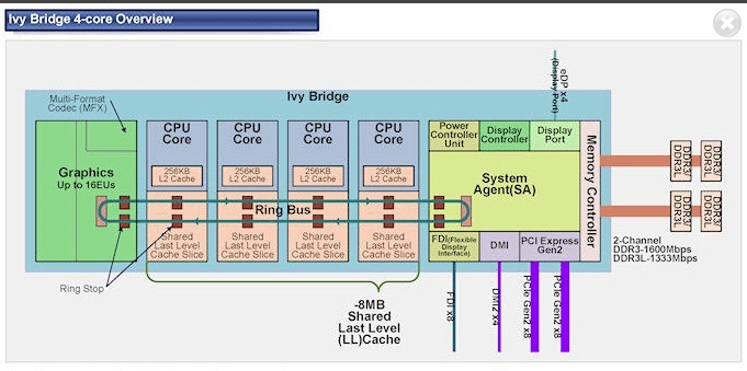
Ivy Bridge has essentially the same layout as Sandy Bridge. The central portion of the die has four x86-64 cores with 256 KB dedicated L2 cache each, and a shared 8 MB L3 cache, while either sides of the central portion has the system agent and the graphics core. All components are bound by a ring-bus, that transports tagged data between the four CPU cores, the graphics core, the L3 cache, and the system agent, which has interfaces for the dual-channel DDR3 integrated memory controller, the PCI-Express controller, and the DMI chipset bus.

Intel can carve four main configurations out of this silicon:
- 4+2: All four cores enabled, full 8 MB L3 cache enabled, all 16 shader cores (EUs) of the IGP enabled
- 4+1: All four cores enabled, 6 MB L3 cache enabled, fewer shader cores of the IGP enabled
- 2+2: Two cores enabled, 4 MB L3 cache enabled, all 16 shader cores of the IGP enabled
- 2+1: Two cores enabled, 3 MB L3 cache enabled, fewer shader cores of the IGP enabled


As mentioned earlier, all components on the silicon are bound by a ring-bus that transports data and instructions between the components. This bus has “ring-stops” from where it picks up and drops off data. The graphics core packs up to 16 programmable EUs that handle parallel processing loads for the GPU, they can also be programmed to perform GPGPU tasks. The system agent holds a dual-channel DDR3 integrated memory controller (IMC), a PCI-Express interface that gives out two x8 ports that can work as a single PCI-Express x16, or switched as two x8 ports; a DMI link to the PCH, a display controller, and FDI link to the PCH. Overall, Intel managed to make more efficient use of its die space.