NVIDIA Unveils Volta GV100 GPU at GTC 2017
Ron Perillo / 7 years ago
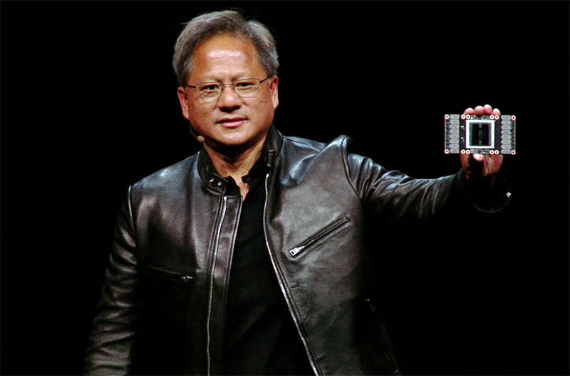
NVIDIA CEO Jen-Hsun Huang showed off what is the next-generation Volta GV100 GPU on the Tesla V100 accelerator during his 2-hour keynote at GTC 2017. The company calls it the “most advanced accelerator ever built”. If this was any other product, that statement would just be a marketing claim. With over 3 Billion dollars spent on R&D, the most the company has ever spent on a project, it is not hard to believe.
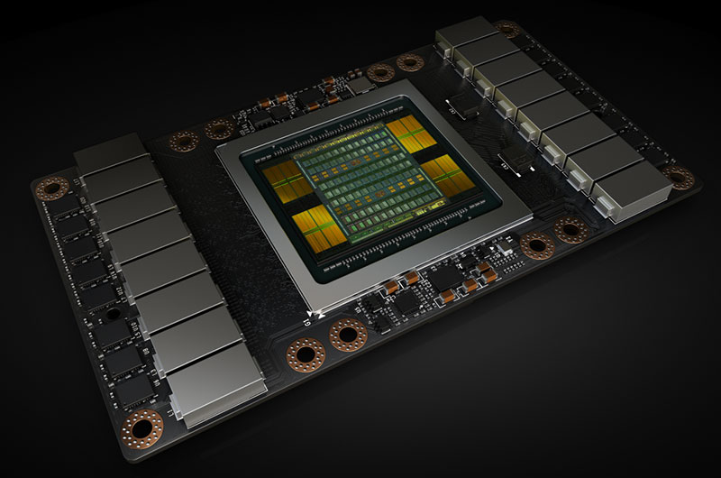
The NVIDIA Volta GV100 GPU is the biggest technological leap from a previous generation in a while. It powers the Tesla V100 accelerator which is the center of NVIDIA’s push for high-performance computing and artificial intelligence convergence. The GV100 GPU itself includes 21.1 billion transistors on a 815 mm2 die size and is fabricated on TSMC’s 12nm FFN high performance process. It utilizes 16GB HMB2 memory from Samsung, delivering 900 GB/sec memory bandwidth. Coupled with the improvements in the memory controller from Pascal, NVIDIA claims 1.5x bandwidth improvement. NVIDIA also upgrades the NVLink to the second generation, now supporting 6 NVLink links at 25GB/s each for a total of 300 GB/s.
NVIDIA Volta GV100 Architecture
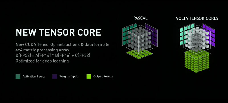
It advances many aspects of computing performance from GPU resource utilization, parallelization, efficiency and pure horsepower over its predecessor. Compared to Pascal, Volta’s SM is 50% more energy efficient. It also uses new “Tensor cores” designed specifically for deep learning, shattering through current standards with over 120 Teraflops. Volta’s peak Teraflops are 5x that of Pascal and 15x over that of Maxwell. It even goes beyond Moore’s Law performance predictions by as much as 4x.
The Pascal GV100 GPU architecture is highly parallelized. Like previous generation Pascal GP100, it is made up of multiple Graphics Processing Clusters (GPC), Texture Processing Clusters (TPCs), Streaming Multiprocessors (SMs), and memory controllers.
A fully unlocked GV100 GPU has six GPCs, 84 Volta SMs, 42 TPCs and eight 512-bit memory controllers (4096 total). Across 84 SMs, there are a total of 5376 FP32 cores, 5376 INT32 cores, 2688 FP64 cores, 672 Tensor Cores and 336 texture units. Each memory controller has a 768 KB L2 cache attached. Even the Tesla V100 accelerator demoed at GTC 2017 only uses 80 SMs and it handily crushed the previous generation performance.

Volta Streaming Multiprocessor
Compared to Pascal, the Volta SM has enhanced L1 data cache and streamlined instruction set. This results in higher performance and lower latency. The new mixed-precision FP16/FP32 Tensor Cores are also purpose-built to handle deep learning arithmetic. It also runs at a higher clocks than Pascal and uses a new partitioning method which improves SM utilization.
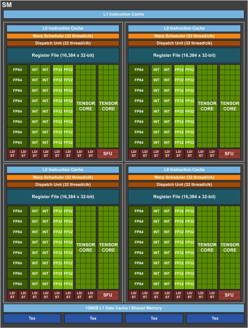
Pascal SMs are partitioned into two processing blocks. Each of these blocks has 32 FP32 cores, 16FP64 cores, an instruction buffer, one warp scheduler, two dispatch units and a 128KB register file.
The new Volta SMs on the other hand, is partitioned into four processing blocks, each with 16 FP32 cores, 8 FP64 cores, 16 INT32 cores, two of the new Tensor Cores, a new L0 instruction cache, a warp scheduler, one dispatch unit and a 64KB register file.
In addition to these changes, Volta can also execute FP32 and INT32 instructions simultaneously, which Pascal could not. Volta also does so at full throughput.
When can we expect NVIDIA Volta gaming graphics cards?
The Tesla V100 with the Volta GP100 GPU is going to be used mostly for HPC applications. Jen-Hsun assuaged attendees of its gaming capability however, with a demo from Square Enix. The demo showed a live rendered scene from Kingslaive: Final Fantasy XV. This particular Square Enix project is a CG movie, but the demo showed the assets rendered in real time. It was rendered in near CG movie quality as well, utilizing NVIDIA’s Gameworks technologies. This included hair simulation, clothing, lighting, etc. The scene was rendered so well live that Jen-Hsun could not help but compliment the character on the screen’s choice of clothing. “That’s a good leather jacket!” he exclaimed while the demo is running. The demo was shown around the 58 minute mark of the keynote.

Following NVIDIA’s history, it might take until Q1 2018 before Volta based video cards make an appearance. That schedule is right around CES 2018 at the earliest. However, rumours have been going around that they are pushing earlier than that date. It will also depend on how well AMD’s Vega performs. If NVIDIA is confident enough that Volta offers a significant performance leap over Pascal, and that consumers will be buying it, then it might be available as early as Q4 or even Q3 2017.