Nvidia GTX 750 Ti 2GB “Maxwell” Graphics Card Review
Ryan Martin / 10 years ago
The Technical Details – Maxwell and GM107
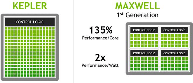
Maxwell uses a very different design to Kepler because it is able to achieve 2X performance per watt and 35% more performance per CUDA core compared to Kepler. We also know that this extra performance has to have come from architectural improvements because both Maxwell (at this stage) and Kepler use the 28nm process, so there are no gains from transistor shrinkage.
Some of the advances the Maxwell design bring include:
- improvements to control logic partitioning
- better workload balancing
- improved clock-gating granularity
- improved compiler-based scheduling
- increased number of instructions issued per clock cycle
The new Maxwell design enables Nvidia to put five SM(M)s into the GM107 which compares to just two SM(X)s in the GK107, that 2.5X increase occurs with just a 25% increase in die area. Another significant improvement is the much larger L2 cache (2048kb in GM107 instead of 256kb in GK107) that allows the graphics card to access the VRAM less frequently resulting in less power consumption and improved performance.
In addition to improving the memory system Nvidia have also improved the integrated H.264 encoder that we first saw on the Kepler GPU. As we know the H.264 encoder allows for Nvidia’s ShadowPlay technology to work, see our review of that here, but it also allows for more effective video playback with reduced power consumption. Maxwell has the capability to provide faster encode and decode thanks to a revised NVENC block; 6-8X real time encode is provided on Maxwell versus 4X on Kepler. There is also 8-10X faster decode due to the addition of new local decoder cache and higher memory efficiency per stream. Finally Maxwell has a GC5 power state specifically designed for light workload cases like video playback. GC5, which some might understand by likening to Intel’s Haswell C6 and C7 states, is a special low power sleep state that provides power savings over older Nvidia GPUs in similar light workload scenarios.
A more detailed explanation of the technicalities in Maxwell is shown below courtesy of Nvidia’s whitepaper:
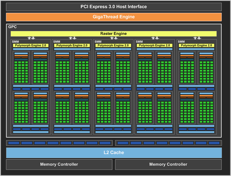
“From a graphics features perspective, our first-generation Maxwell GPUs offer the same API functionality as Kepler GPUs. At the high level, Maxwell also implements multiple SM units within a GPC (Graphics Processing Cluster), and each SM includes a Polymorph Engine and Texture Units, while each GPC includes a Raster Engine. ROPs are still aligned with L2 cache slices and Memory Controllers. Internally, all the units and crossbar structures have been redesigned, data flows optimized, power management significantly improved, and so on.
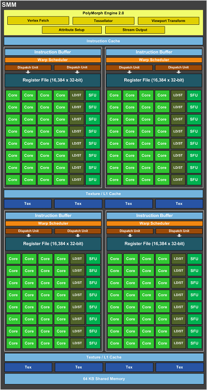
The GM107 GPU contains one GPC, five Maxwell Streaming Multiprocessors (SMM), and two 64-bit memory controllers (128-bit total). This is the full implementation of the chip, and is the same configuration we ship with the GeForce GTX 750 Ti.The primary contributor to Maxwell’s improved efficiency is the new Maxwell SM architecture, SMM. This new SM architecture achieves much higher power efficiency and delivers 35% more performance per CUDA Core on shader-limited workloads. Achieving these results required a number of major changes to the architecture. The SM scheduler architecture and algorithms have been rewritten to be more intelligent and avoid unnecessary stalls, while further reducing the energy per instruction required for scheduling.
The organization of the SM has also changed. Each SM is now partitioned into four separate processing blocks, each with its own instruction buffer, scheduler and 32 CUDA cores. The Kepler approach of having a non-power-of-two number of CUDA cores, with some that are shared, has been eliminated. This partitioning simplifies the design and scheduling logic, saving area and power, and reduces computation latency.
Pairs of processing blocks share four texture filtering units and a texture cache. The compute L1 cache function has now also been combined with the texture cache function, and shared memory is a separate unit (similar to the approach used on G80, the first CUDA capable GPU), that is shared across all four blocks. Overall, with this new design, each “SM” is significantly smaller while delivering about 90% of the performance of a Kepler SM, and the smaller area enables us to implement many more SMs per GPU. Comparing GK107 versus GM107 total SM related metrics, GM107 has five versus two SMs, 25% more peak texture performance, 1.7 times more CUDA cores, and about 2.3 times more delivered shader performance.”