TSMC Announces Wafer-on-Wafer 3D Stacking Technology
Ron Perillo / 6 years ago
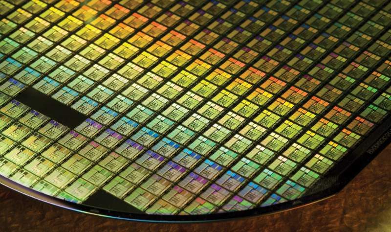
Wafer-on-Wafer Packaging
Taiwan Semiconductor Manufacturing Company Ltd (TSMC), the world’s largest chip contract manufacturer in the world is announcing their new 3D stacking technology called Wafer-on-Wafer (WoW).
This technology builds upon TSMC’s Chip-on-Wafer-on-Substrate (CoWoS) and Integrated Fan-Out (InFO) 3D manufacturing. You might have not heard of these words before, but you have most definitely used hardware which uses them. The second generation InFO technology for example is used on the iPhone’s A11.
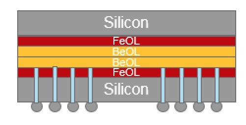
Specifically, the WoW process stacks two flipped wafers together, starting with the silicon level outside and continues beyond the front end of line and back end of line. The matching wafer has to be mirrored for this to work since they have to align.
As for how the wafers communicate, one wafer uses Through-Silicon Vias (TSVs) for the I/Os. If you notice, it is working on the wafer level so that means these are bonded at a much earlier process. Which also means the yields have to be much higher in order to compensate for the bad wafers that have to be discarded. Bad wafer bonded with a good wafer means it is thrown out completely.
Does This Mean Stacked GPUs in the Future?
Maybe if you travel far enough into the future. However, it does not look like this TSMC packaging tehcnology is for GPU stacking. This would be more ideal for mobile or other lower-power applications where the RAM can stack on the SoC.
Bigger dies like CPUs and GPUs can get similar bandwidth improvements through an interposer or interconnect instead. For example such as Intel’s EMIB or AMD’s HMB/HBM2 usage. That is without adding thermal problem generated from physically stacking. Keep in mind that the silicon facing the FeOL layer also gives way to the TSVs. This means another die has to be underneath. Which increases the already high chance of defects and further increasing the cost.
7nm+ and 5nm On the Way
WoW is not the only announcement TSMC made. They are also announcing a 7nm improvement called 7nm+ and that 5nm is well-on schedule. Unfortunately for gamers, this is once again not for GPUs. Rather these will find home on advanced mobile and high-performance computing (HPC). 5nm is on track for Q1 2019, and 3nm is not too far away either. Especially with the 3nm-specific fab building starting in 2020.